Electronic products even today consist of traditional plastic molded housings containing PCB’s with soldered THT and SMT components. Design of a product is based on the electronics that should fit inside. Next step is to design where electronics are part of the design based on ergonomics and aesthetics?
This can be done by placing electronics in way inside the design. Target is eliminating separate piece of FR4 material.
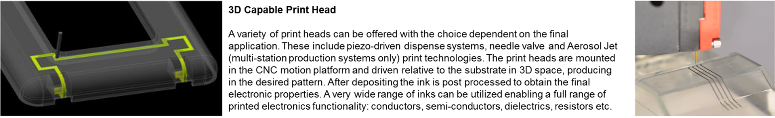
Neotech’s 3D Printed Electronics technology is based on combination of three key modules – Motion 3D Tool-path Generation Software, 5 axis CNC Motion Platform and 3D Capable Print Head for optimized Hard- and Software package.
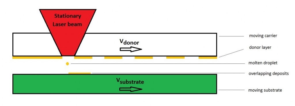
Laser Induced Forward Transfer (LIFT) uses laser to shoot small droplets of conductive material (Dimensions 1-10 μm) from a carrier onto a substrate as shown in the below picture. Deposition size is typically smaller than the hole in the donor layer. Further, the substrate and the donor both move with respect to the laser beam, each with their own velocity to create overlapping deposits which form a conducting line.
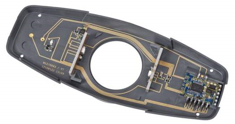
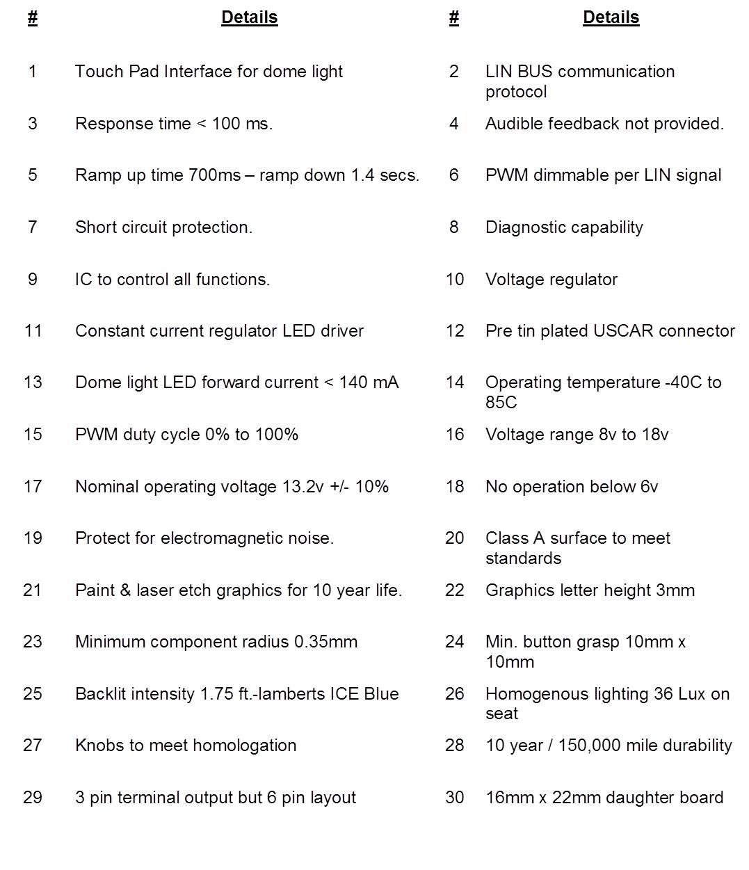
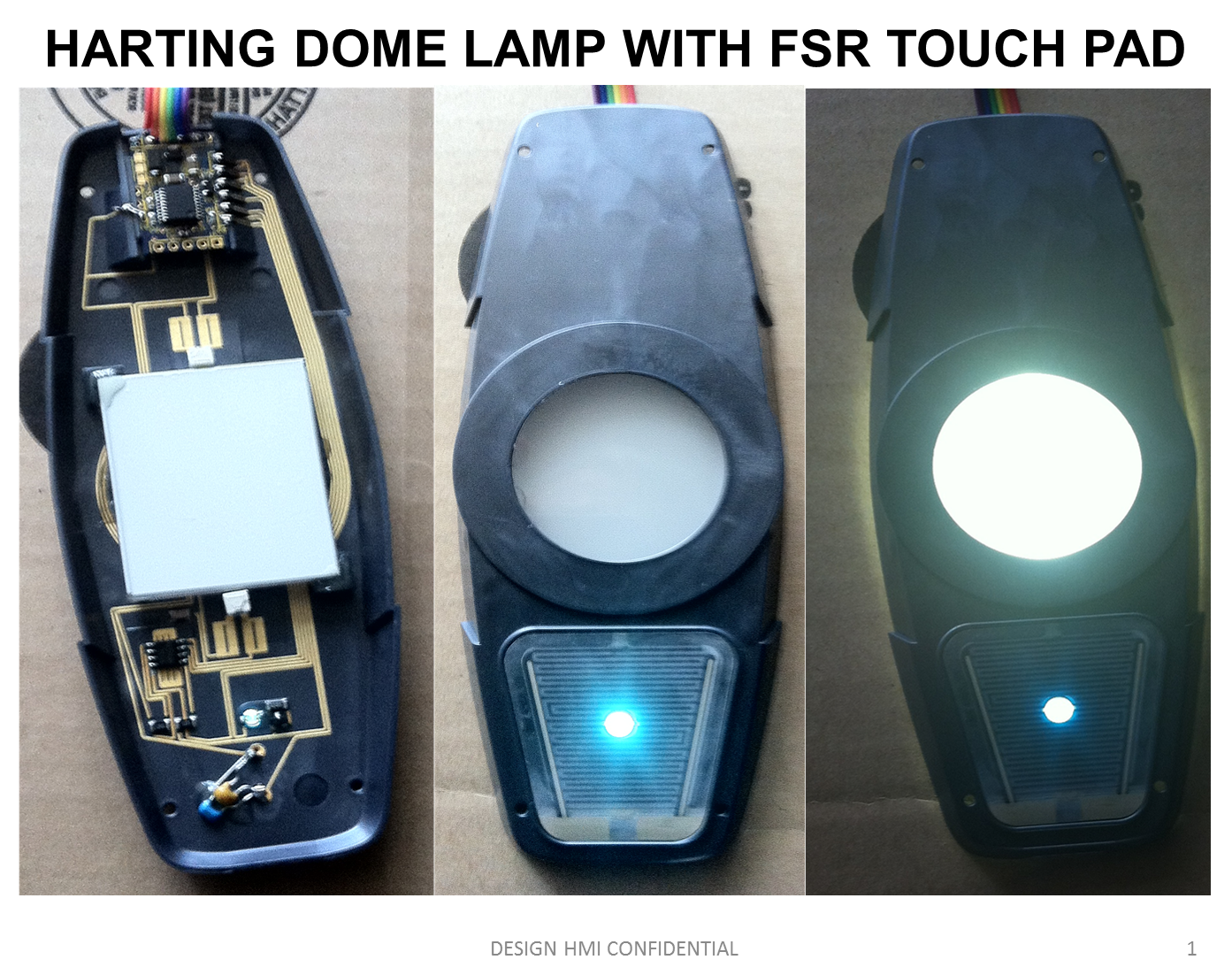
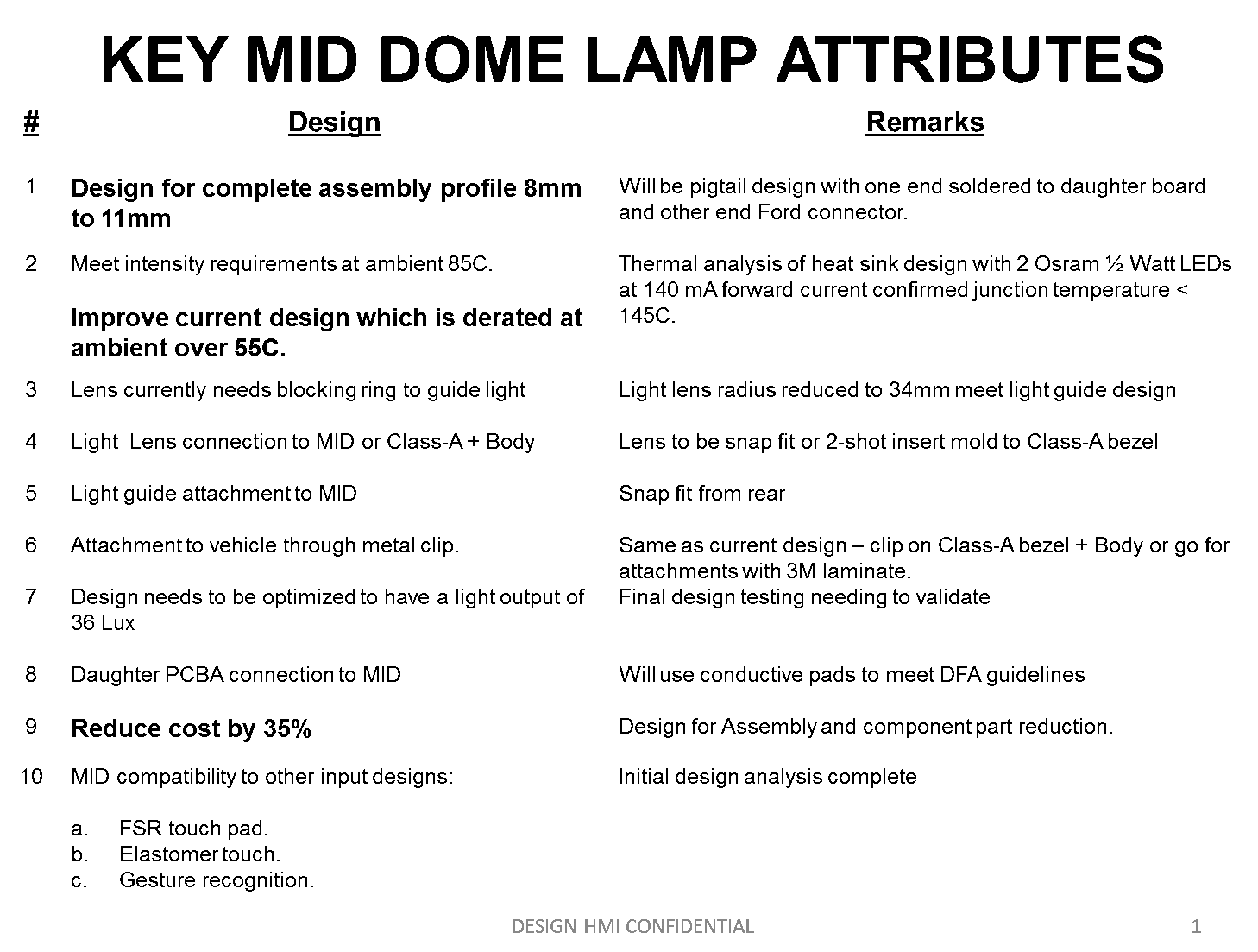
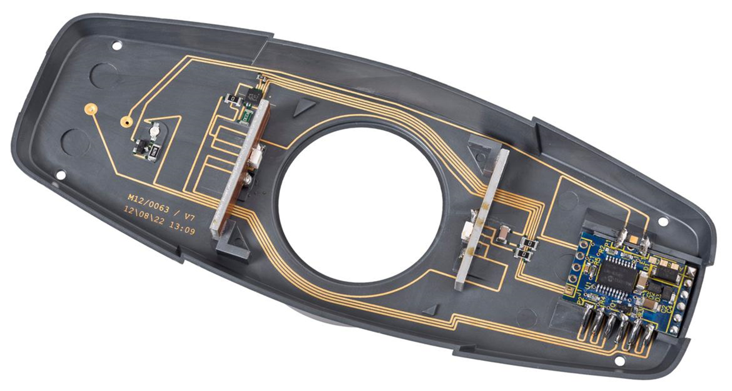
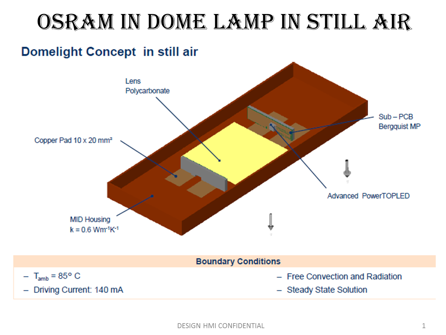
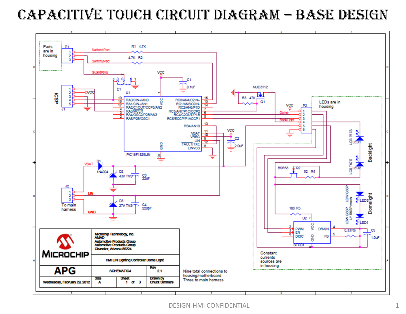
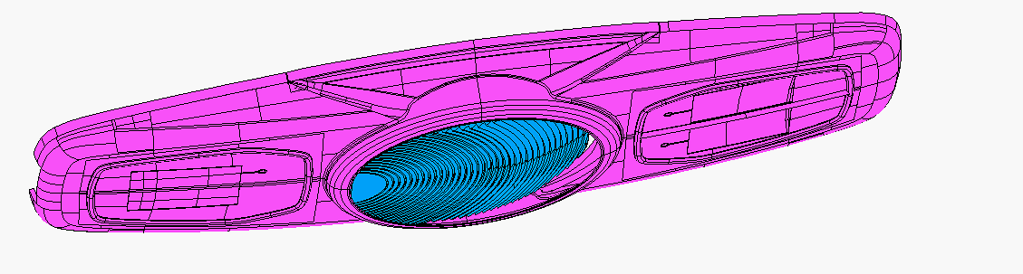
Molded Interconnect Dome Lamp designed in partnership with OSRAM, Microchip Electronics, IEE SA and Harting SA.
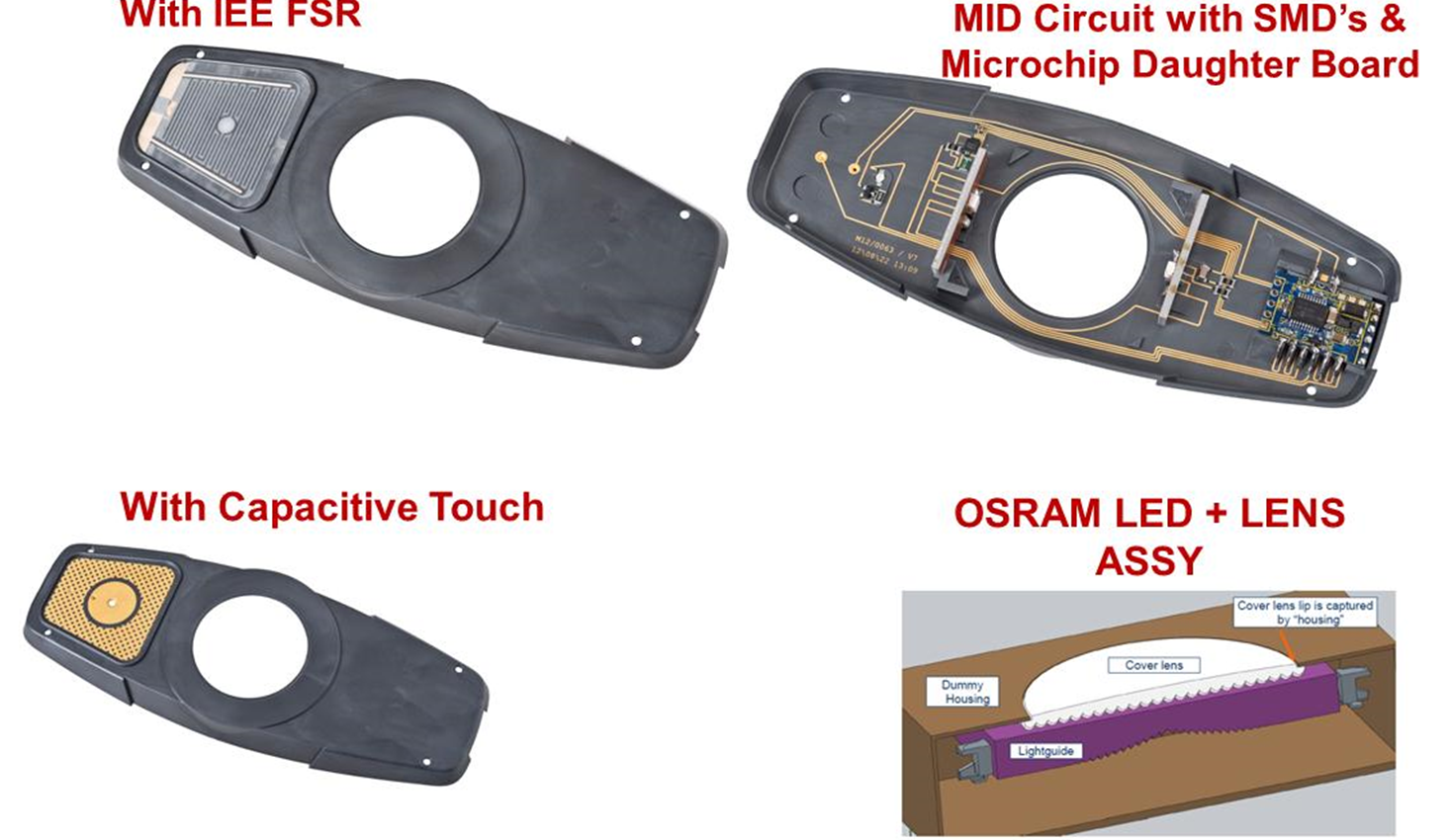
Design target as below:
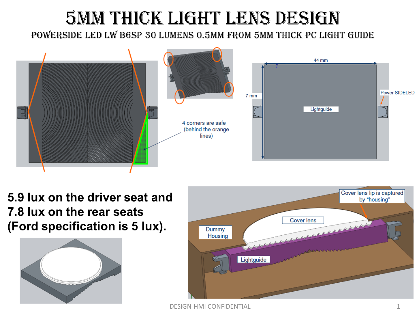
- Low profile of between 8mm to 11mm.
- Design for application with moon roof and as hidden light applications.
- Drop in replacement to Ford 2012 MY packaging & system interface.
- Common lighting for dome lamp and reading lamp with higher intensity.
- Work at temperature extreme of 850C.
- Provide touch interface.
- LIN Bus interface.
- Theater dimming.
- Direct cost target $4.00 to $6.00 for 35% reduction cost reduction.
- Component reduction for improved reliability.
For more information contact designhmi@gmail.com
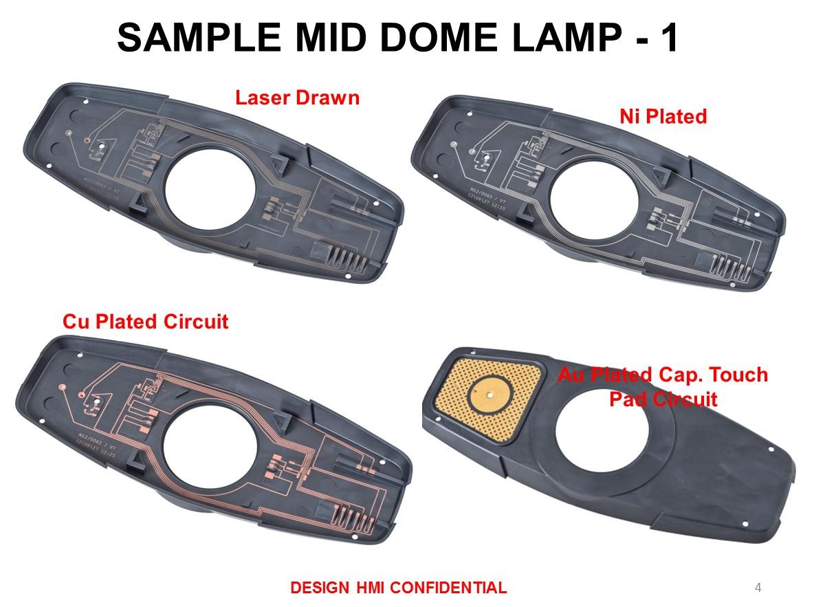
Definition of MID Technology:
- 3D means solutions in three dimensions are possible
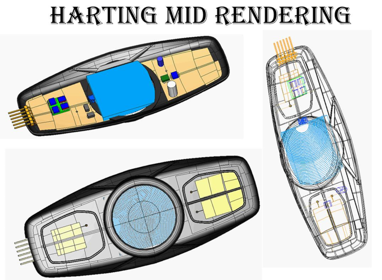
- MID means Molded Interconnect Device
- A 3D circuit is realized by structuring the metal layers
- Simply speaking – a three-dimensional PCB is created
- Reduced system volume
- Packaging solutions require only small foot print on PCB
- 3D features are integrated in process, no additional cost
- Molding process guarantees high precision and high repeatability
- Laser structuring allows easy design changes
For more information contact:
http://www.harting-mitronics.ch/en.html