
DuPont In Mold Electronics (IME) Ink for Automotive Electronic Circuits
Automotive HMI & Smart Trim Applications
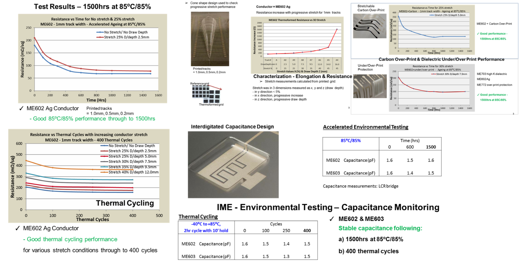
DuPont ME603 and ME602 Silver Conductors
DuPont advancements in electronic ink combines stretchable 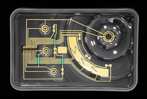 material with ink to give interface designers new creative freedom. DuPont new electronic inks work with existing in-mold decorative processes not requiring re-tooling.
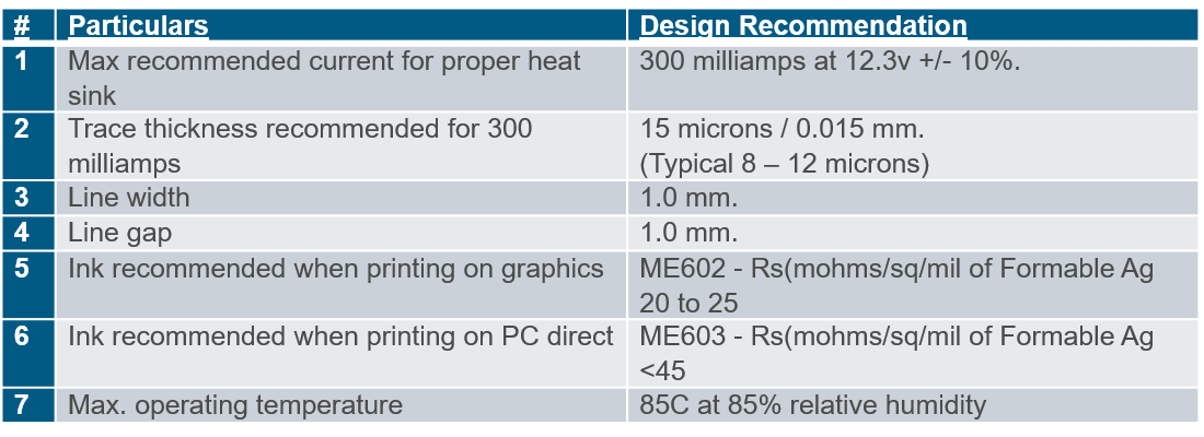
Working on the assumption that 300 milliamps at 12.3v are also trying to develop recommendations for:
- Ink usage on circuit length of length of 30 mm.
- Estimated cost of printing.
This would allow to develop engineering estimate for different applications and determine business case for application.
A few process recommendations:
Mounting Components: This can be done before thermoforming on flat surface or after thermoforming into 3D shape with pick and place machine.
Base Material: DuPont ink has been tested our materials on a subset of PC films – none are particularly special. Recommend DuPont ME 603 for this application.
Circuits on Graphic Ink: If graphic ink (decorative) layer is printed on the PC film prior to printing IME materials interface to the graphic ink layer can be more important than the PC. Recommend DuPont ME 602 for these applications.
Insert Molding: When insert molding thermoformed assemblies with LEDs and resistors it is assumed they have encapsulate material applied to them before “insert molding”. As they are already designed to survive lead free solder temperatures they should survive insert molding temperatures. Gate design may be important in some cases.
Thermoforming: Performance of ME603 is dependent on design. If more precision is needed with printed symbols and structures, high pressure forming has shown to give more accuracy as it ensures more even stretch. Forming temperatures around 160°C can be used.
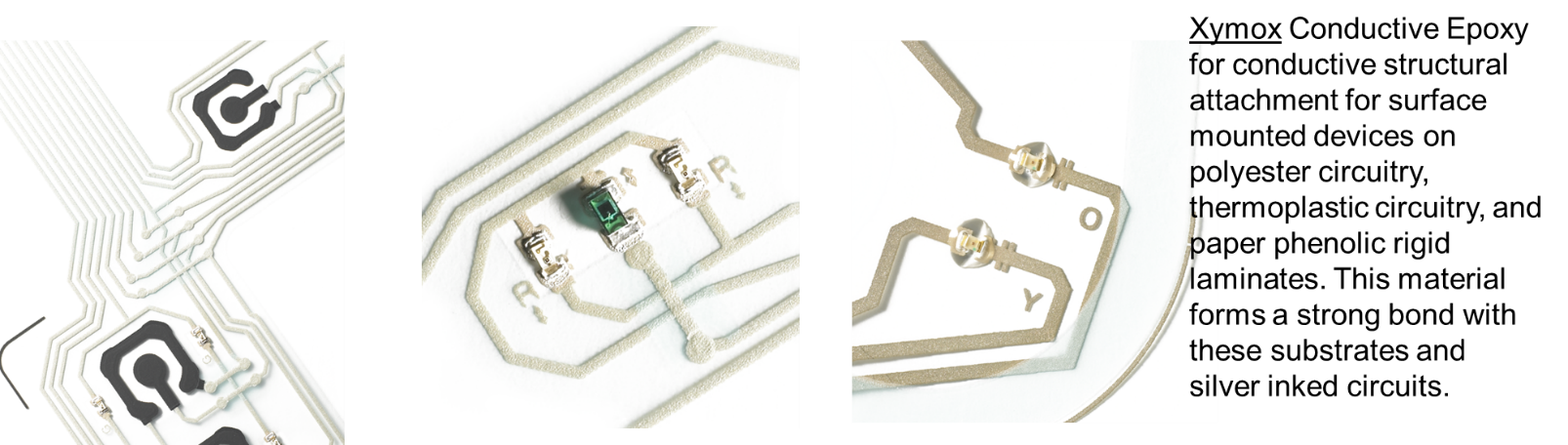
Electrically Conductive Adhesives (ECA): The liquid ECA is applied in liquid form at room temperature onto the circuit pads using a dispensing system.
Dry in a well-ventilated box oven or belt/conveyor furnace. Air flow and extraction rates should be optimized to ensure complete removal of solvent from the paste. A strong air flow may help to reduce the drying temperature combination. It will also aid in achieving the lowest as-printed resistance.
Typical Drying Conditions in box oven are 120°C for 20 minutes and reel-to-reel 120°C for 4 minutes
Soldering SMD Components: The discrete parts to be “glued on” the circuit are placed onto the circuit pads with the liquid ECA. The entire part is then heated to the curing temperature of the ECA material (120C for our materials) for a given time (typically 4 minutes) in a well-ventilated belt dryer.
Alternatively, the curing of the parts with ECA can be done in a box oven, 120C for 20 minutes.
Circuit Current: DuPont typical conductive silver materials have a resistivity specification of ~35 mohms/square/mil, and this should be used to calculate the resistance of the conductive traces.
LED Circuits: Standard small chip LED biased at 3.3V and ~20 mA, a 0.040″ wide conductive trace of a few inches length would have a series resistance of <10 ohms
If application requires multiple of these LEDs and equal luminance is critical, care might need to be taken in the layout design to keep the series resistances of the traces equal, for example.
At this stage would not recommend high current functional LEDs (> 150 mA each) as head sink would become critical factor. IME circuit on PC does not make good heat sink.
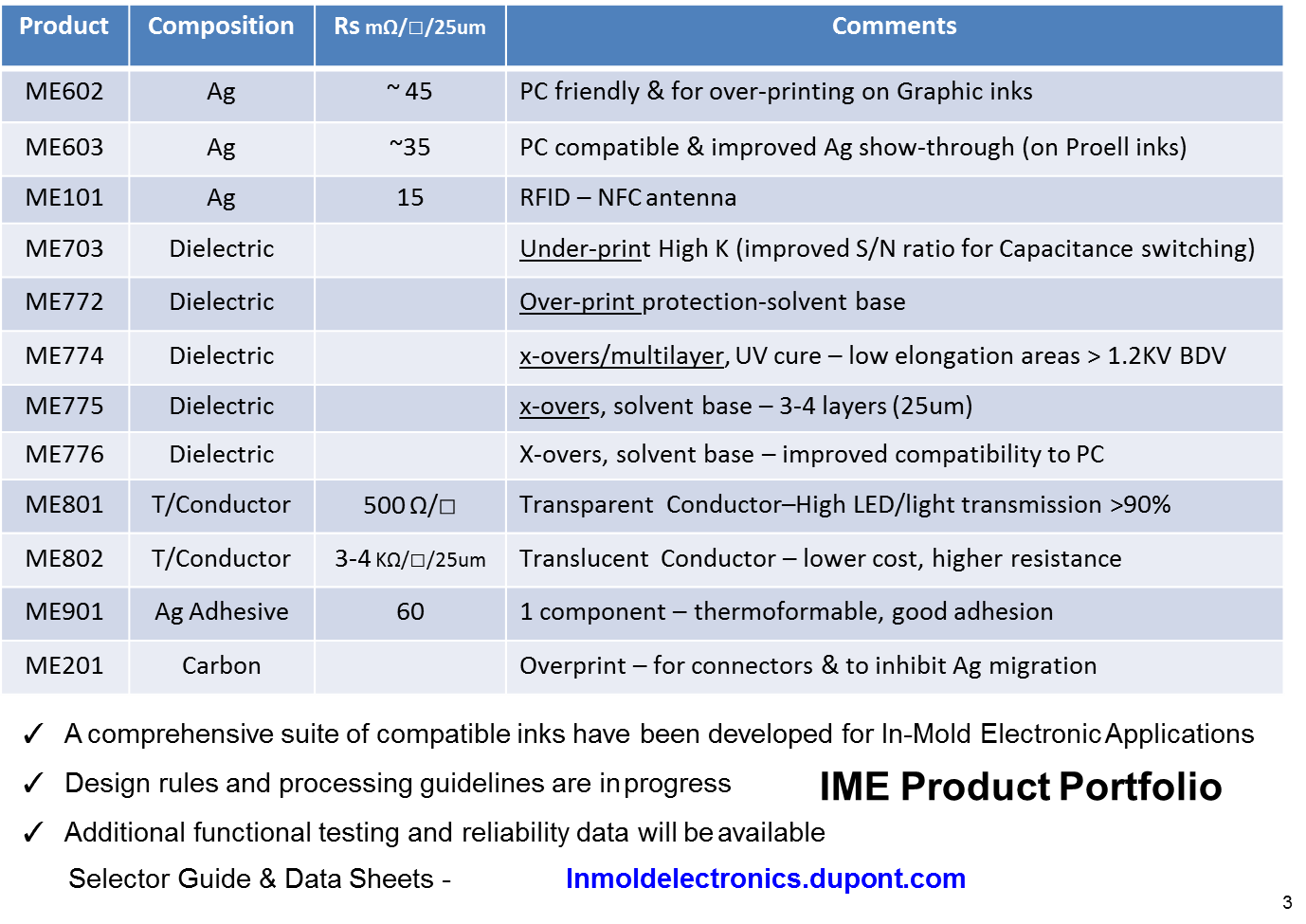
DuPont manufactures a suite of conductive pastes that are used to create the in-mold electronic circuit.
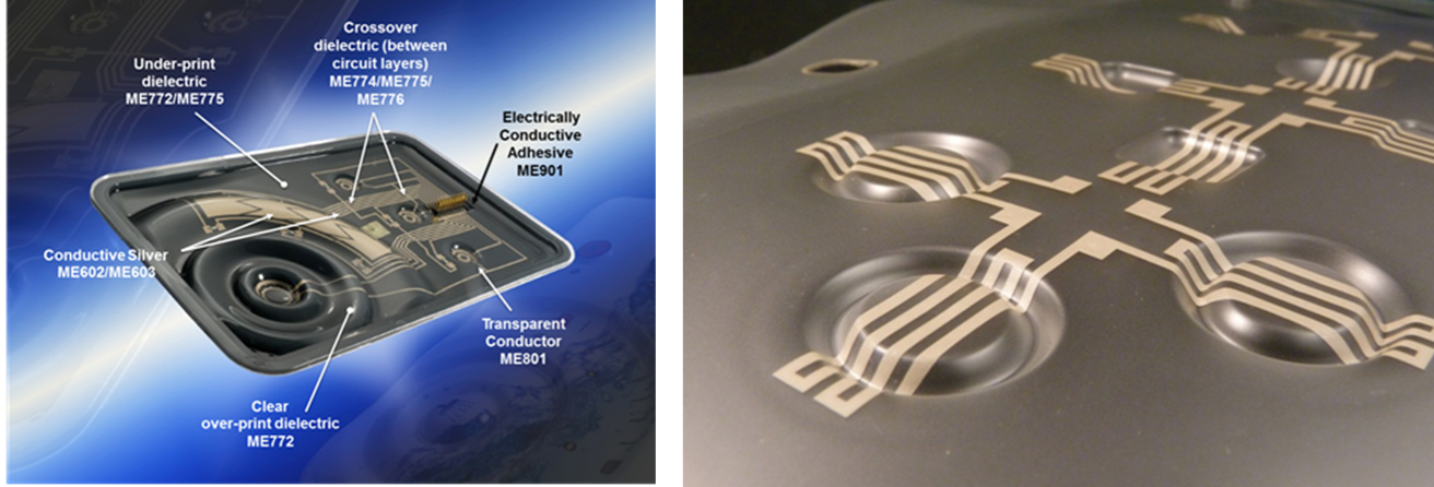
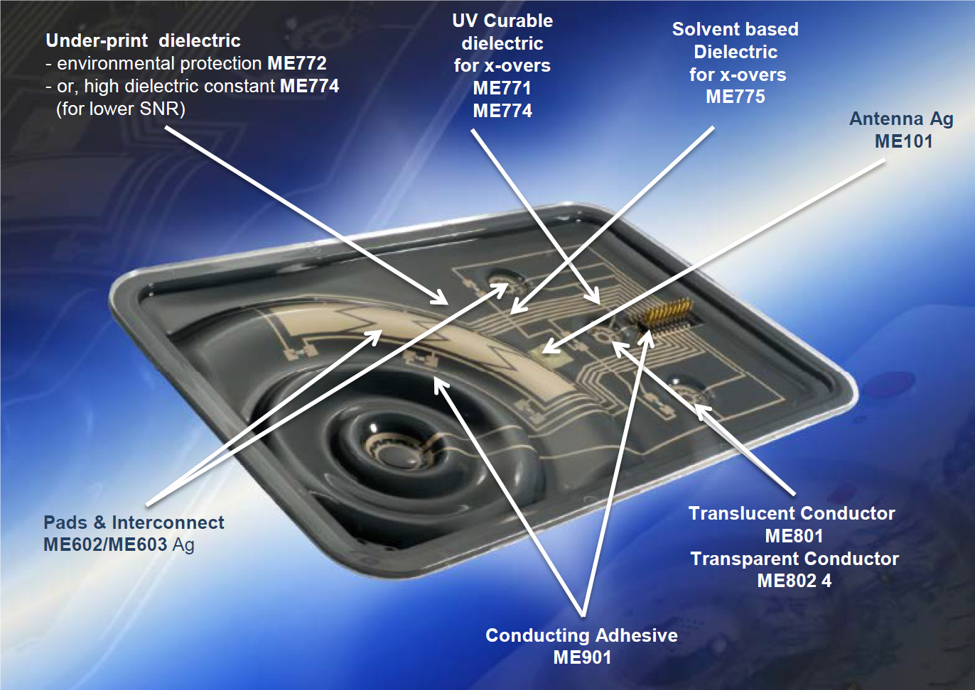
ME101 is developed for In Mold Electronic applications suited for RFID applications. ME101 is a silver conductive ink capable of withstanding thermoforming and over molding temperatures.
ME201 is carbon conductive ink capable of withstanding thermoforming and over molding temperatures.
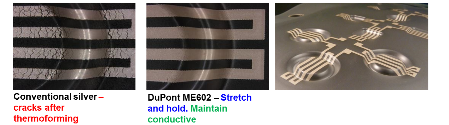
ME602 is a stretchable silver conductor capable of withstanding thermoforming and over molding temperatures for Capacitive Switch applications and interconnecting circuitry enabling fully integrated 3-dimensional functional electronic devices.
ME603 is a stretchable silver conductor capable of withstanding thermoforming and over molding temperatures for capacitive Switch applications and interconnecting circuitry enabling fully integrated 3-dimensional functional electronic devices.
Again, benefits are higher conductivity silver for In Mold Electronics, minimal/no silver show-through on graphics layer, adhesion directly on polycarbonate and graphic inks and performance after thermoforming and injection molding.
Substrates can be Polycarbonate
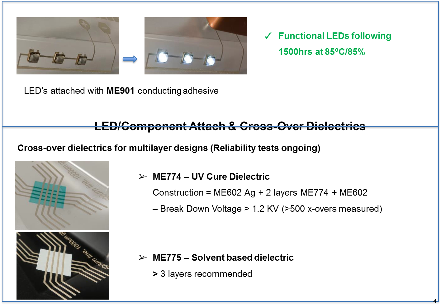
ME775 is a solvent based crossover dielectric capable of withstanding thermoforming and over molding temperatures. This composition is intended to be used for high elongation Capacitive Switch applications.
ME901 is a stretchable silver conductive adhesive capable of withstanding thermoforming and over molding temperatures. This composition can be used to attach LEDs and build capacitive switches on polycarbonate substrates coated with graphic inks and/or over glaze.
Typical Circuit Line Thickness is 1 Micron printed with SD 56/36 (280mesh) stainless steel or 77 – 48 PET Screen.
Inks are:
- Flexible, conductive silver composition for In Mold Electronics.
- Adhesion directly on Polycarbonate.
- Designed to meet functional requirements after thermoforming and injection molding.
Suited for Polycarbonate and Surface Treated Polyester substrates. Screen printing can be Reel-to-reel, semi-automatic or manual. Typical Drying Conditions for box oven are 120°C for 20 minutes and for reel-to-reel 120°C for 4 minutes. Clean-Up Solvent is Ethylene diacetate.
After printing, ME101 will interact with polycarbonate if left wet for extended periods. It is therefore recommended to dry as soon as possible after printing. Drying is a critical processing step and to achieve optimum performance, sufficient temperature/time should be allowed to ensure complete removal of solvent.
Dry in a well-ventilated box oven or belt/conveyor furnace. Air flow and extraction rates should be optimized to ensure complete removal of solvent from the paste. A strong air flow may help to reduce the drying temperature combination. It will also aid in achieving the lowest as-printed resistance.
Example of Stack-up Guidelines – 2 conductor & 2 dielectric layers
- Trace Widths: 0.025” minimum with space between traces is typically 0.025” minimum.
- In 2 conductor designs with crossovers, increase bottom conductor trace widths by at least 0.010” to create landing area for top conductor to account for miss-registration.
- Start of landing area on trace should be 0.100” from top crossover.
- Cross-over dielectric is a minimum of 0.020” to 0.040” wider than trace on each side.
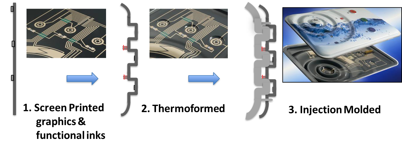
In-Mold Electronics refers to Printed Electronic Circuitry, on film, which has undergone thermoforming and injection molding process. The circuit remains functional as the conducting tracks contour the 3D shape.
This technology is can be considered an extension / addition to IMD/FIM (Film Insert Molding) – base technology from the 1990’s. Essentially combines film, graphics and electronics to form a 3D functional fully integrated electronic device with components.
Now this innovation has been developed by others over the last 10 years. DuPont ME602 conductor survive intense stretching and heat of the thermoforming and injection molding process with good adhesion.
DuPont ME series paste can be used to construct true 3D circuits with capacitive switches and LED lighting for applications in automotive, aviation and appliances.
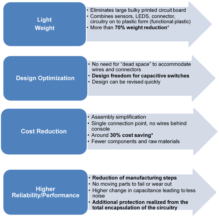
Application allows assembly to be 70% lighter and Buttons and 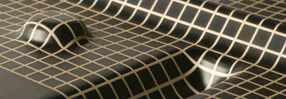 wires are eliminated, removing most of the weight from a typical assembly.
Up to 30% less cost, simpler and more efficient production. Part assembly time cut by 40% single-connection reduces assembly time while increasing reliability and ease of service.
New design freedom whether with Capacitive LED switches, Piezo or others which can be arrayed anywhere, in virtually any shape.
Flexible Hybrid Electronics or In Mold Electronics is a technology being pursued for application by all major 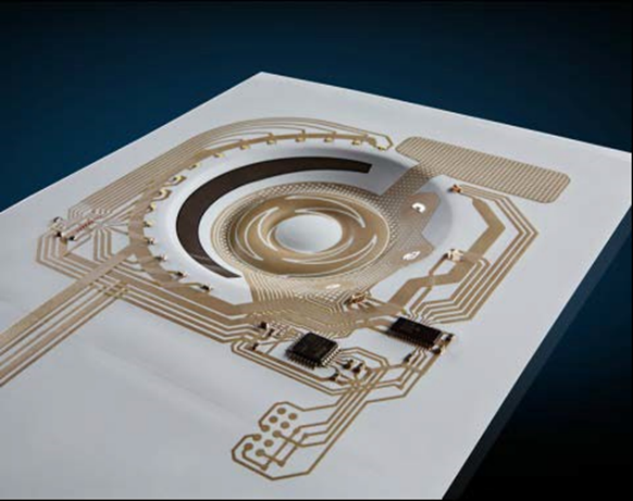 companies for the last 15 years. However in the last three / four years only has there been real progress among North American companies.
DuPont is a key innovator in this area.
Benefits of In-Mold Electronics
DuPont has Complete Solution for In-Mold Electronics:
- Suite of patented IN Mold-Electronic materials
- Growing database of compatible materials (films, graphic inks, LEDs, Controllers, processes, and converters)
- Working demo
- Design rules
- Manufacturing rules
- Cost comparisons vs. not in-kind technologies
- Functional and reliability data
- Base interconnect technology (connector)
- Industry know-how
For More Information, contact www.duPont.com
For more information contact Dupont contact Vince Arancio, Senior technical specialist– vince.arancio@dupont.com or Dave Hui ,Business development manager, West region – dave.hui@dupont.com.
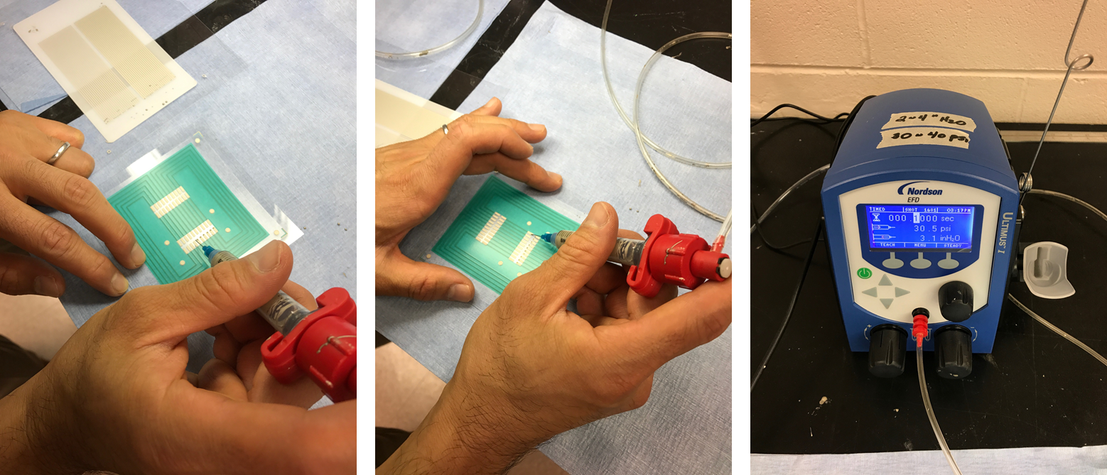
Conductive Glue Dispensing Recommendation and Pick & Place Equipment
For circuits on plastic or in mold electronics the process is as follows:
- Circuits are printed.
- Conductive glue is dispensed.
- SMD components are placed on the circuit.
- The process is completed through high temperature chamber to activate the glue.
There are specific production methodologies for the process but below are two recommendations for prototype equipment to dispense the conductive glue and pick & place the SMD components.
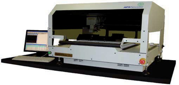
LE40V Benchtop Automated Pick & Place with Vision Centering:
- Placement rate of Placement rates up to 3000 cph with accuracy ±0.001”.
- Place virtually all SMT components from 0201 discreets, ultra-micro BGAs, CSPs, and 15 mil pitch QFPs
- Easy to use Windows ® based software for panelized boards, self-diagnostics, error recognition, fault monitoring and more.
- Standard self-contained vacuum eliminates need for costly external air source
- Cognex ® Vision System with fiducial correction, bad board mark, and pattern recognition
- Handle loose and tube components with the optional vibratory feeder with frequency and amplitude control
- Conveniently use short tape strips with their SuperStrip™ feeders in 8, 12, 16, 24, 32, 44, and 56mm.
Nordson Ultimus I-II Dispensers features a digital display of all fluid dispenser settings and time adjustment as fine as 0.0001 seconds, Ultimus™ I-II dispensers bring exceptional control to medical device, electronics, and other critical dispensing processes.
Ultimus I feature 0-100 psi (0-7 bar) constant-bleed air pressure regulation and provides greater control when dispensing any type of fluid.
Ultimus II features 0-15 psi (0-1 bar) constant-bleed air pressure regulation and provides greater control when dispensing low-viscosity or thin fluids.
Features
- All-digital, multi-function display
- 16 memory settings
- 4-decimal time setting
- Operator lockout of time setting
- Multilingual display options
- Universal power supply
There are various conductive ink coatings to print circuits on different surfaces – mainly ITO films.
Most of these applications are for touch screens designed to form a low-resistance transparent conductive layer with high optical characteristics.
Conductive inks contain pigments that provide function, beyond that of color and substrate hiding power of graphic inks. Conductive components contained in conductive inks may be comprised of silver, carbon, graphite, or other precious metal coated base material. Depending on the application, more exotic conductive fillers exist.
Conductive inks can be applied in several ways including screen print, flexographic or rotogravure, spray, dip, syringe dispense, and stencil print. Conductive inks are formulated for a specific method of application. Conductive inks for screen printing tend to be solvent based because water based inks evaporate too quickly and the viscosity tends to be too low to screen effectively. Water- based inks are available for high speed printing and coating applications (refer Applied Ink Solutions).
Challenge: Print conductive film over curved surfaces on which SMD components can be soldered using conductive glue with current carrying capacity of 500 mA for LED currents and components needed to drive LED’s.
The other application is printed electronics for cost and manufacturing efficiency to produce circuitry on a printing press creating a product that is flexible also offers new opportunities and form factors.
A study was published in Journal of Nanoparticle Research 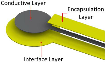 based on Aqueous silver nanowire inks consisting of AgNW (length of 30 μm, and diameter of 40 and 90 nm) on rheological behavior and structure depend on shear and temperature. Is worth reading for ink innovators.
Dupont screen printable inks include: DuPont 7723, a low temperature firing silver ink suitable for printing on glass, and DuPont 9169, a low temperature curing Ag ink designed for flexible substrates.
Creative Materials fine line inks are capable of line widths and spaces as small as 50 to 75 microns and is RoHS compliant.
Direct-write technologies can form a low-cost alternative  approach to create interconnects by eliminating mask and etch costs as well as by being more efficient at low area coverage and high aspect ratio. Existing direct write technologies, either a metallic ink or paste, typically containing Nano-Particles, is used or an ink containing precursor for electroless plating. Metallic inks containing nanoparticles always require a thermal or photonic treatment to achieve sintering, hence electrical conductivity. Plating precursors need an (electro)less plating step to create the actual track. Hence, such precursor printing only solves part of the problems associated with the conventional approach.
To be able to write structures compatibly with advanced IC packaging approaches, a deposition resolution of 1-5 μm is required.
The following are some typical process technologies:
- Laser-induced forward transfer (LIFT) method exists where material is transferred from a supported thin film to a receiver substrate by irradiating the rear side of the film with a single laser pulse.
- Inkjet printing can be used in electronics packaging as interconnections between electronic components. Conductive inks and dielectric inks are used when substituting traditional printed circuit board (PCB) with inkjet-printed interconnections.
- Aerosol Jet Printing is another material deposition technology for printed electronics. The Aerosol Jet process begins with atomization of an ink, which can be heated up to 80°C, producing droplets on the order of one to two microns in diameter. The atomized droplets are entrained in a gas stream and delivered to the print head. Resulting patterns can have features ranging from 10 microns wide, with layer thicknesses from 10’s of nanometers to >10 microns.
- 3D MID technology (Molded Interconnect Devices) is another way to create an electrical interconnect inside a molded plastic housing. An electrical conductive circuit is created by means of two-shot molding or by laser activation patterning. After this step the structures get metallized through an electroless plating process and become conductive.
Challenge: Soldering LED’s for both ambient and functional lighting where current could be as high as 450 mA at 12v, Heat sink both for heat loss in voltage regulator as well LED’s will need to be designed.
Approximately 70 percent is converted to heat while only 30 percent of the energy passing through an LED chip is converted to light. This affects reliability and the color temperature of the LED. LED chip manufacturers try to keep the junction temperature within the semiconductor at 75-85°C, which allows more light output from the device along with better light color and longer life. With more thermally conductive substrates, there is the potential capability to use fewer LED die in a design to get the desired light output.
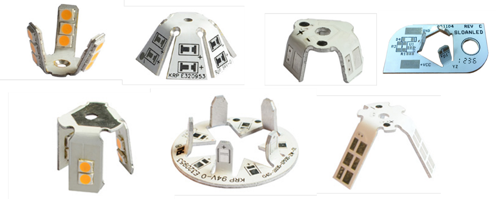
By replacing thick FR-4 boards with metal-core laminate boards (MCBs) such as DuPont™ CooLam™ thermal substrate, heat dissipates from the LED faster due to the thin dielectric material.
DuPont has developed acrylic and polyimide technologies to meet the needs of industries as varied as aerospace, automotive and consumer electronics. Forty years ago, the company introduced its Kapton® polyimide film technology, and subsequently Pyralux® flexible circuit materials. Polyimides possess a unique combination of properties that make them ideal for a variety of applications in many different industries. The ability of polyimide to maintain its excellent physical, electrical, and mechanical properties over a wide temperature range has opened new design and application areas. It has excellent chemical resistance; there are no known organic solvents for the film. Polyimide has the highest UL-94 flammability rating – V-0 – and does not melt or burn. Its outstanding properties permit it to be used at both high and low temperature extremes where most other organic polymeric materials would not be functional.
CooLam™ thermal substrates were developed for use in sub mount, chip-on-board, and metal core PCB LED packaging applications. These thermal-clad laminates are a composite of metal foil and proprietary thermally conductive polyimide dielectric bonded to a metal base, and they provide an ideal insulated metal substrate for high-brightness LED lighting.
The Munich-based WACKER chemicals group has developed a 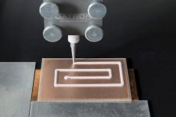 thermally conductive adhesive for electronics applications. The new silicone rubber with the trade name SEMICOSIL® 975 TC is characterized by high thermal conductivity and good flow and processing properties
This may be used to print circuits on thermally conductive adhesive with SEMICOSIL® 975 TC acting as a heat sink.
.
